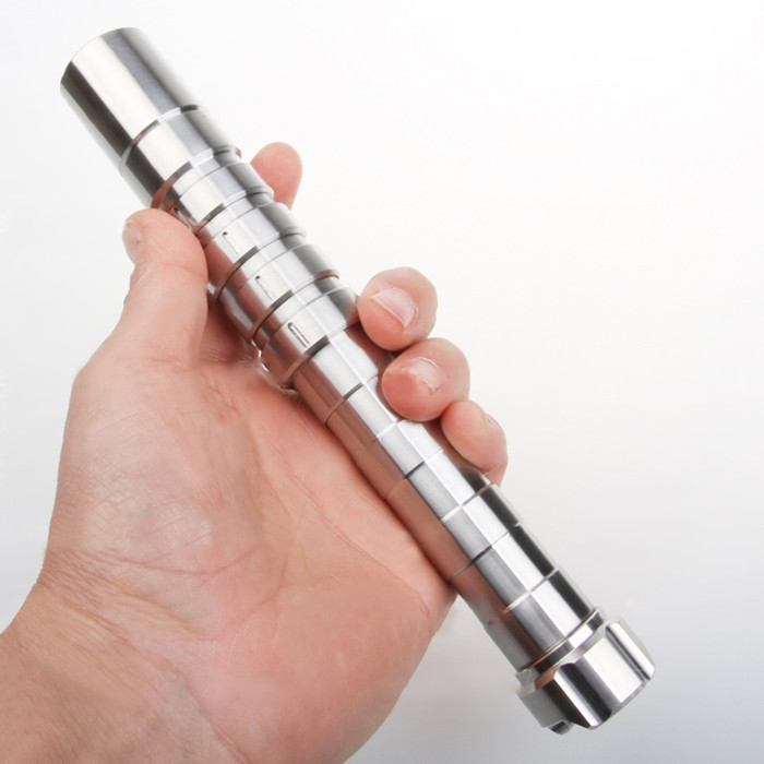
3W, 5W, 10W, 15W, 20W, 30W… The power of UV laser pointer is also the same as fiber lasers, which has been constantly breaking through. With the increase in power, the application fields of ultraviolet lasers with many performance advantages such as narrow pulse width, multiple wavelengths, large output energy, high peak power and good material absorption have become wider and wider.
Ultraviolet laser is not only widely used, but also used in the fine processing of various materials such as plastics, glass, metals, ceramics, PCBs, cover films, silicon wafers, etc., but also deeply applied, which is multiple manufacturing of a single material Equipment responsible for the process. Taking PCB manufacturing as an example, ultraviolet lasers are used in multiple processes such as cutting, etching, and drilling.
1. Responsible for PCB cutting
In covering film cutting, PCB mass cutting and disassembly (removing a single circuit board from the panel), UV lasers are currently the best choice.
The cover film constitutes the insulating area between the assembly components of the multilayer circuit board, which is used for environmental isolation and electrical insulation, and protects fragile conductors. It needs to be cut according to a specific shape, and the use of a fine ultraviolet laser can avoid damaging the release paper, so that the formed covering film can be easily separated from the release paper. Flexible or rigid-flex PCB materials are very thin. UV laser can not only eliminate the influence of mechanical stress generated during the disassembly process, but also greatly reduce the influence of thermal stress.
2. Responsible for PCB etching
The process of PCB from the light board to showing the circuit pattern is a complicated process, among which, etching is required. Compared with the chemical etching of the pattern plating method, the ultraviolet blue laser pointer etching is faster and more environmentally friendly. At the same time, the UV laser spot size can reach 10μm, and the etching accuracy is higher.
3. Responsible for PCB drilling
Multi-layer PCBs are made of composite materials by hot die-casting together to form semi-cured parts, which are easy to separate when exposed to high temperatures. The UV laser with the reputation of “cold” processing can therefore flex its muscles. Ultraviolet laser technology is widely used in the production of micropores with a diameter of less than 100μm. With the use of miniature circuit diagrams, the pore size can even be less than 50μm. Ultraviolet laser technology produces very high yields when making holes with a diameter of less than 80μm.
In order to meet the increasing demand for micro-hole productivity, many manufacturers have begun to introduce dual-head UV laser drilling systems.
4. More responsibility
In recent years, the demand for laser precision machining in 3C electronics and other industries has risen rapidly, driving the development of ultraviolet laser engraver. According to statistics from the Optical Industry Research Center, the number of UV lasers shipped was more than 6,000 in 2016, more than 9,000 in 2017, soared to 15,000 in 2018, and 19,000 in 2019. It can be seen that ultraviolet lasers have become an important force in the manufacturing industry. With the continuous localization of UV lasers, the competition between domestic and foreign brands will be further strengthened, which objectively helps the further popularization of UV lasers in domestic laser processing.
